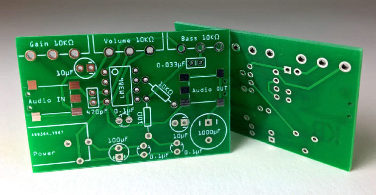
Everybody talks about software these days. Products 3G, 4G, 5G cell phones, Smart TV’s, Navigation Systems, Space technology, robotics, automotive, Aerospace are the discussion points. All talk and discuss the software and user-friendly features of the product. What they do not know is that you need hardware to write or develop the software. The heart of the product is the Printed Circuit Board (PCB). PCB board design from companies like avanticircuits.com is the first step in achieving that goal.
So what is PCB board design? Take any electronic product the heart, is the printed circuit board. It is fundamental in any electronic product. An electronic product without a printed circuit board means nothing. Electronic components, circuit design, placement, interaction, paths are required. All together on a single layer board or a multi-layer board gives birth to the PCB. The PCB board design definition – is coming together of factors to have a working output as per technical specifications is PCB board design. The board needs to be a non-conductor of electricity. Fiber or glass are common materials for PCB board design. “FR4” fiber is popular.
What are the building blocks in a PCB board design? The starting point – schematic diagram. It needs capturing. A schematic capture tool is required. At this stage lot of simulations can be done to optimize the design. Radio Frequency (RF) circuits, which are the most complex, benefit from the simulation. Prototype generation eliminated, saving cost. The output of schematic capture is the netlist. Netlist details the paths and interconnectivity of the components.
Component placement the next step in PCB board design. The designer needs to have a rough idea. RF components need placing in a separate area. The component placement provides input to how many PCB layers are required. The estimation of footprints, holes, drilling, pads are cleared with it.
An important step that follows is routing. It connects all the components. The exact number of layers finalization completes. Separate layers for ground and power planes are required. Prevent interference problems. Noise level reduction and low source resistance are benefits. Routing consumes time. An experienced engineer or technician needs a requirement for this job with the proper tools. A lot of things can go wrong in PCB board design if the routing quality is inefficient.
Trace width is another factor to be considered. The traces determine how the components are connected. Current consumption reduces due to proper trace width design. The majority of copper traces bend at a 45-degree angle. 90-degree angle cause signal reflection in high-speed digital logic circuits. File generation and drilling information follow. Photo plot output used in the manufacturing process. Gerber file outputs are popular.
Today, technology growth takes place at a rapid pace. Miniaturization is key. PCB board design increase in complexity. Several tools are available for PCB board design. Eagle, Multisim, CAD software commonly used for schematic layout design. Electronic Design Automation (EDA) or Electronic Computer-Aided Design (ECAD) find use. Choose the right tool for your application. Remember that every step in PCB board design is critical to creating a game changer product.


Comments are closed.